- 您现在的位置:买卖IC网 > Sheet目录492 > NTMS4937NR2G (ON Semiconductor)MOSFET N-CH 30V 8.6A 8SOIC
�� �
�
�NTMS4937N�
�Power� MOSFET�
�30� V,� 13.6� A,� N� ?� Channel,� SO� ?� 8�
�Features�
�?� Low� R� DS(on)� to� Minimize� Conduction� Losses�
�?� Low� Capacitance� to� Minimize� Driver� Losses�
�?� Optimized� Gate� Charge� to� Minimize� Switching� Losses�
�?� These� Devices� are� Pb� ?� Free,� Halogen� Free/BFR� Free� and� are� RoHS�
�Compliant�
�http://onsemi.com�
�Applications�
�?� DC� ?� DC� Converters�
�?� Points� of� Loads�
�?� Power� Load� Switch�
�?� Motor� Controls�
�MAXIMUM� RATINGS� (T� J� =� 25� °� C� unless� otherwise� stated)�
�Parameter� Symbol�
�Drain� ?� to� ?� Source� Voltage�
�V� DSS�
�Gate� ?� to� ?� Source� Voltage�
�V� GS�
�Value�
�30�
�±� 20�
�Unit�
�V�
�V�
�V� (BR)DSS�
�30� V�
�R� DS(ON)� MAX�
�6.5� m� W� @� 10� V�
�8.7� m� W� @� 4.5� V�
�N� ?� Channel�
�D�
�I� D� MAX�
�13.6� A�
�Continuous� Drain�
�Current� R� q� JA� (Note� 1)�
�Power� Dissipation� R� q� JA�
�(Note� 1)�
�Continuous� Drain�
�Current� R� q� JA� (Note� 2)�
�Steady�
�State�
�Steady�
�State�
�Steady�
�State�
�T� A� =� 25� °� C�
�T� A� =� 70� °� C�
�T� A� =� 25� °� C�
�T� A� =� 25� °� C�
�T� A� =� 70� °� C�
�I� D�
�P� D�
�I� D�
�11.2�
�9.0�
�1.36�
�8.6�
�6.9�
�A�
�W�
�A�
�G�
�S�
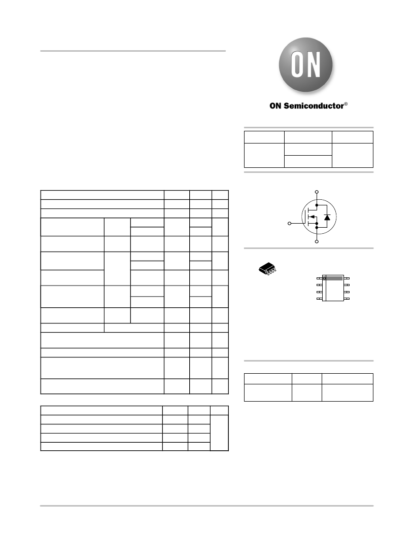
�MARKING� DIAGRAM/�
�PIN� ASSIGNMENT�
�Source�
�Source�
�Gate�
�Power� Dissipation� R� q� JA� T� A� =� 25� °� C�
�(Note� 2)�
�Continuous� Drain� Steady� T� A� =� 25� °� C�
�Current� R� q� JA� ,� t� v� 10� s� State�
�(Note� 1)� T� A� =� 70� °� C�
�Power� Dissipation� Steady� T� A� =� 25� °� C�
�R� q� JA� ,� t� v� 10� s(Note� 1)� State�
�Pulsed� Drain� Current� T� A� =� 25� °� C,� t� p� =� 10� m� s�
�Operating� Junction� and� Storage� Temperature�
�P� D�
�I� D�
�P� D�
�I� DM�
�T� J� ,�
�T� stg�
�0.81�
�13.6�
�11�
�2.0�
�112�
�?� 55� to�
�150�
�W�
�A�
�W�
�A�
�°� C�
�1�
�1� Source�
�SO� ?� 8�
�CASE� 751�
�STYLE� 12�
�Top� View�
�4937N� =� Device� Code�
�A� =� Assembly� Location�
�Y� =� Year�
�WW� =� Work� Week�
�G� =� Pb� ?� Free� Package�
�8�
�Drain�
�Drain�
�Drain�
�Drain�
�Source� Current� (Body� Diode)�
�Single� Pulse� Drain� ?� to� ?� Source� Avalanche� Energy�
�(T� J� =� 25� °� C,� V� DD� =� 30� V,� V� GS� =� 10� V,�
�I� L� =� 13� A� pk� ,� L� =� 1.0� mH,� R� G� =� 25� W� )�
�Lead� Temperature� for� Soldering� Purposes�
�(1/8� ″� from� case� for� 10� s)�
�I� S�
�E� AS�
�T� L�
�2.1�
�84.5�
�260�
�A�
�mJ�
�°� C�
�(Note:� Microdot� may� be� in� either� location)�
�ORDERING� INFORMATION�
�Device� Package� Shipping� ?�
�NTMS4937NR2G� SO� ?� 8� 2500/Tape� &� Reel�
�THERMAL� RESISTANCE� MAXIMUM� RATINGS�
�(Pb� ?� Free)�
�Parameter�
�Junction� ?� to� ?� Ambient� –� Steady� State� (Note� 1)�
�Junction� ?� to� ?� Ambient� –� t� v� 10� s� (Note� 1)�
�Junction� ?� to� ?� Foot� (Drain)�
�Junction� ?� to� ?� Ambient� –� Steady� State� (Note� 2)�
�Symbol�
�R� q� JA�
�R� q� JA�
�R� q� JF�
�R� q� JA�
�Value�
�91.9�
�61.1�
�22.6�
�154.7�
�Unit�
�°� C/W�
�?For� information� on� tape� and� reel� specifications,�
�including� part� orientation� and� tape� sizes,� please�
�refer� to� our� Tape� and� Reel� Packaging� Specification�
�Brochure,� BRD8011/D.�
�Stresses� exceeding� Maximum� Ratings� may� damage� the� device.� Maximum�
�Ratings� are� stress� ratings� only.� Functional� operation� above� the� Recommended�
�Operating� Conditions� is� not� implied.� Extended� exposure� to� stresses� above� the�
�Recommended� Operating� Conditions� may� affect� device� reliability.�
�1.� Surfacemounted� on� FR4� board� using� 1� in� sq� pad� size� (Cu� area� =� 1.127� in� sq�
�[1� oz]� including� traces).�
�2.� Surfacemounted� on� FR4� board� using� the� minimum� recommended� pad� size.�
�?� Semiconductor� Components� Industries,� LLC,� 2009�
�September,� 2009� ?� Rev.� 0�
�1�
�Publication� Order� Number:�
�NTMS4937N/D�
�发布紧急采购,3分钟左右您将得到回复。
相关PDF资料
NTMS4N01R2G
MOSFET N-CH 20V 3.3A 8-SOIC
NTMS5835NLR2G
MOSFET N-CH 40V 9.2A 8SOIC
NTMS5838NLR2G
MOSFET N-CH 40V 7.5A 8SOIC
NTMS5P02R2SG
MOSFET P-CH 20V 3.95A 8SOIC
NTMS7N03R2
MOSFET N-CH 30V 4.8A 8-SOIC
NTMSD2P102LR2G
MOSFET P-CH 20V 2.3A 8-SOIC
NTMSD3P102R2G
MOSFET P-CH 20V 2.34A 8-SOIC
NTMSD3P303R2G
MOSFET P-CH 30V 2.34A 8-SOIC
相关代理商/技术参数
NTMS4939N
制造商:ONSEMI 制造商全称:ON Semiconductor 功能描述:Power MOSFET 30 V, 12.5 A, N−Channel, SO−8
NTMS4939NR2G
功能描述:MOSFET Power MOSFET 30V 100A 8.4 mOhm Single RoHS:否 制造商:STMicroelectronics 晶体管极性:N-Channel 汲极/源极击穿电压:650 V 闸/源击穿电压:25 V 漏极连续电流:130 A 电阻汲极/源极 RDS(导通):0.014 Ohms 配置:Single 最大工作温度: 安装风格:Through Hole 封装 / 箱体:Max247 封装:Tube
NTMS4N01R2
功能描述:MOSFET 20V 4.2A N-Channel RoHS:否 制造商:STMicroelectronics 晶体管极性:N-Channel 汲极/源极击穿电压:650 V 闸/源击穿电压:25 V 漏极连续电流:130 A 电阻汲极/源极 RDS(导通):0.014 Ohms 配置:Single 最大工作温度: 安装风格:Through Hole 封装 / 箱体:Max247 封装:Tube
NTMS4N01R2/D
制造商:未知厂家 制造商全称:未知厂家 功能描述:Power MOSFET 4.2 Amps, 20 Volts
NTMS4N01R2G
功能描述:MOSFET 20V 4.2A N-Channel RoHS:否 制造商:STMicroelectronics 晶体管极性:N-Channel 汲极/源极击穿电压:650 V 闸/源击穿电压:25 V 漏极连续电流:130 A 电阻汲极/源极 RDS(导通):0.014 Ohms 配置:Single 最大工作温度: 安装风格:Through Hole 封装 / 箱体:Max247 封装:Tube
NTMS4P01R2
功能描述:MOSFET P-CH 12V 3.4A 8-SOIC RoHS:否 类别:分离式半导体产品 >> FET - 单 系列:- 标准包装:1,000 系列:MESH OVERLAY™ FET 型:MOSFET N 通道,金属氧化物 FET 特点:逻辑电平门 漏极至源极电压(Vdss):200V 电流 - 连续漏极(Id) @ 25° C:18A 开态Rds(最大)@ Id, Vgs @ 25° C:180 毫欧 @ 9A,10V Id 时的 Vgs(th)(最大):4V @ 250µA 闸电荷(Qg) @ Vgs:72nC @ 10V 输入电容 (Ciss) @ Vds:1560pF @ 25V 功率 - 最大:40W 安装类型:通孔 封装/外壳:TO-220-3 整包 供应商设备封装:TO-220FP 包装:管件
NTMS4P01R2/D
制造商:未知厂家 制造商全称:未知厂家 功能描述:Power MOSFET -4.5 Amps, -12 Volts
NTMS5835NL
制造商:ON Semiconductor 功能描述:MOSFET N CH W DIO 40V 9.2A 8SO 制造商:ON Semiconductor 功能描述:MOSFET, N CH, W DIO, 40V, 9.2A, 8SO